

Highlight
High-Performance Transistors from the World's Thinnest Material
Single-atom-thick transistors
Achievement/Results
Single-atom-thick sheets of graphite — so-called “graphene” films — have incredible electrical and mechanical properties that could revolutionize many fields. Since the films conduct electricity very easily, some researchers have hypothesized that graphene would be the ideal material for fast, high-performance transistors. On the atomic scale, graphene’s honeycomb lattice resembles atomic-scale chicken wire. In spite of this seemingly open structure, the films are completely impervious to atoms, but essentially transparent to light and electrons. Can these ultrathin films be used as perfect windows, perhaps allowing high-tech electron microscopes that only operate in vacuum to see into the watery environment of a living cell?
These properties and others have captured the imagination of scientists around the world, but one problem has kept these dreams from becoming a reality. Graphene films are thinner and more delicate than a soap bubble. How can these extremely delicate films be cut, stretched, positioned, and “glued” in place without damage?
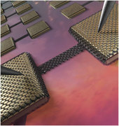
Working with a team of interdisciplinary engineers and scientists at Cornell University, IGERT Fellow Mark Levendorf has developed a simple technique that can reliably cover entire silicon wafers with hundreds upon hundreds of graphene devices. Using a recipe developed by other workers, they first grow a graphene film across an entire copper-covered wafer. Borrowing techniques from the microelectronics industry, they then cut the film into the desired shapes and remove the excess graphene. In the final step, they use a special solution to remove the underlying copper from select regions of the wafer, allowing the now unsupported film to gently drape down onto the underlying wafer without wrinkling or creasing. Using this new technique, Levendorf and coworkers fabricated large arrays of graphene transistors with a 97% success rate.
The simplicity and high-yield of this new method are, in principle, suitable for industrial-scale mass production of graphene-based devices. Is a new generation of high-performance electrical and mechanical devices just around the corner?
M. P. Levendorf, C. S. Ruiz-Vargas, S. Garg and J. Park, Nano Letters 9, 4479 (2009).
Address Goals
Discovery: The development of new techniques for the high-yield fabrication of graphene-based devices will enable both fundamental research on the properties of this amazing material, as well as the development and characterization of new nanoscale electrical and mechanical devices that are predicted to have transformative properties. Potential applications range from high-performance nanoscale electronic devices to high-resolution electron and scanned probe microscopies.
Learning: This highly interdisciplinary and integrative research project required the sustained contributions of scientists and engineers with a wide range of talents and expertise. This project required contributions from chemists to enables the production of monolayer thick films, from nanoscale engineers to precisely shape and cut the films, and from materials scientists to characterize the film’s structure and properties. This interdisciplinary milieu provided an ideal training ground for next-generation scientists and engineers educated in cutting-edge nanoscience.
