
Highlight
Efficient Thin Film Solar Cells via Nanocrystal Ink Route
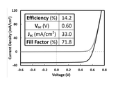
JV curve for a 14.2% efficient C1GSSe Solar Cell via Nanocrystal Route
Achievement/Results
We have developed a nanocrystal ink-based route for Cu(In,Ga)S2 (CIGS) and Cu2ZnSnS4 (CZTS) based thin film solar cells. This device fabrication method represents a promising, low-cost technology due to the minimal amounts of raw materials required and the potential for scalability to large-scale production. The sintering of CIGS and CZTS nanocrystal films into dense, micron-sized grains in a selenium atmosphere at 450-600 °C and the resulting substitution of S with Se in the crystal lattice – a process known as selenization – is one of the key steps in device fabrication that is poorly understood. However, recent interdisciplinary collaborations between Purdue University and Helmholtz-Zentrum Berlin für Materialien und Energie (HZB) under the Solar Economy IGERT (SEIGERT) program have led to the design and execution of novel experiments to elucidate the selenization mechanism. Utilizing HZB equipment, Purdue materials, and expertise from materials scientists, physicists, and chemical engineers, energy-dispersive x-ray diffraction (EDXRD) analysis was performed for CIGS and CZTS selenization procedures in real time at the BESSY II synchrotron facility in Berlin, Germany.
The collected data reveal previously undetected reaction pathways in the selenization mechanism, indicating a transition through copper selenide as a key initiator for grain growth and sulfide-to-selenide conversion in films of both materials. The attached figure depicts representative EDXRD data collected during the selenization of CZTS nanocrystals. The peaks labeled ∑1 and ∑2 correspond to the 112 crystal planes in the sulfide CZTS and the resulting selenized CZTSe films, respectively. A transitional copper selenide phase is clearly observed, and its disappearance coincides with the appearance of ∑2, suggesting the two events are correlated. Along with an improved understanding of the selenization mechanism, a new champion efficiency of 14.2% has been achieved for devices fabricated from CIGS nanocrystals. This value represents a benchmark efficiency for similarly processed nanocrystal-based solar cells. Ultimately, studying the mechanism of absorber layer sintering through the Purdue/HZB collaboration has led to improved understanding of the growth of high quality, thin film solar cell absorber layers by leveraging the unique capabilities, expertise, and equipment contributed by both parties.
Address Goals
Primary Strategic Goal: Understanding the Sintering of the Semiconducting nanoparticles into large micronsize grains is a key fundamental aspect for creating efficient solar cells. When and why do these nanoparticles sinter or do not sinter? What factors lead to sintering from the top surface or the bottom surface for both? How is the sandwiched layer of submicron grains formed and what will it take to eliminate it? The observations so far are very different from the typical sintering knowledge in material science. Therefore, our research is providing fundamental knowledge in the process of sintering of the semiconducting nanoparticles. Secondary Strategic Goal: The research is being conducted by trainees from different disciplines of engineering and science. It is cultivating world-class trained individuals with interdisciplinary knowledge that is essential for the future workforce. The trainees are poised to contribute to the workforce needed for the emerging renewable energy field.