
Highlight Photo
Development of Processes Needed to Grow Single Crystal Silicon Nanowires from a Self-Assembly Patterned Array
Fig 1 Schematic of the etch-transferred features with a gold film
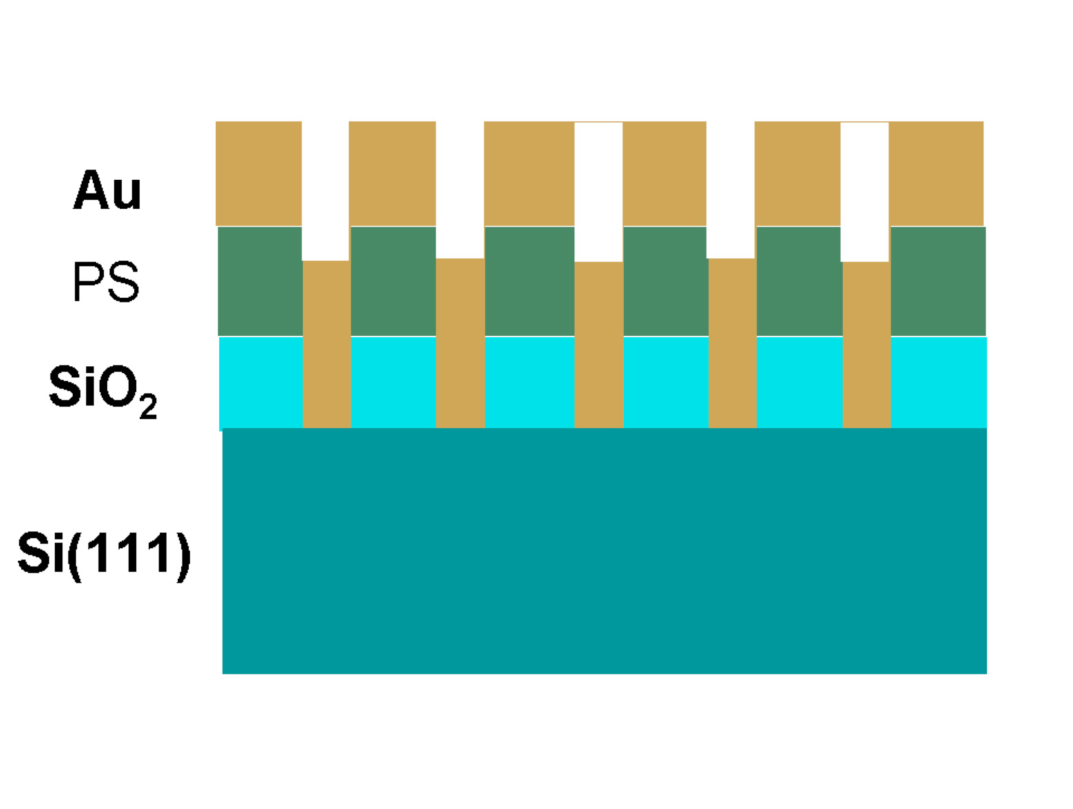
Figure 1. Schematic of the etch-transferred features with a gold film.
Credits: Benjamin Spivey and John Ekerdt