
Highlight Photo
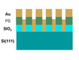
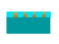
Development of Processes Needed to Grow Single Crystal Silicon Nanowires from a Self-Assembly Patterned Array
Fig 3 Scanning electron microscope image
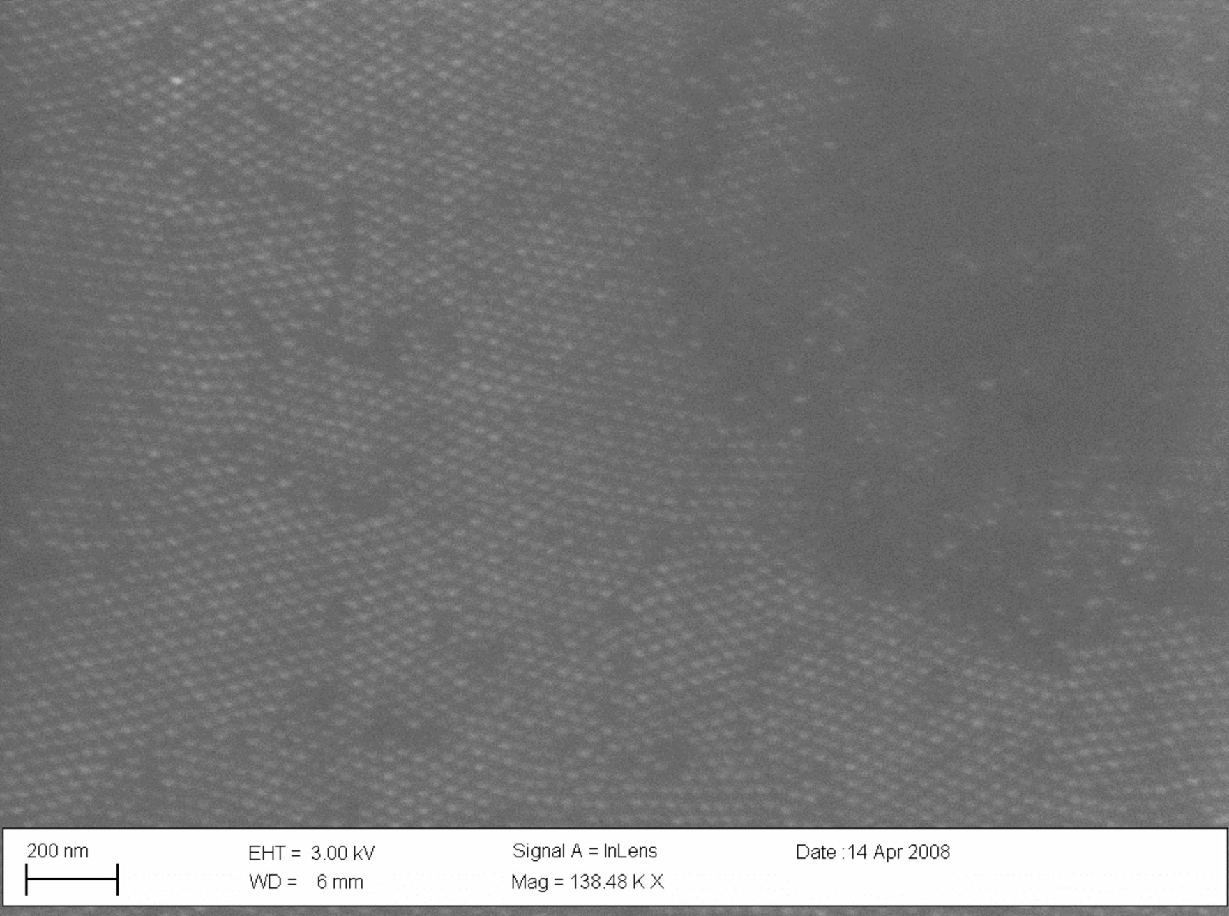
Figure 3. Scanning electron microscope image of a lift-off region showing the ordered Au nanoparticles at in the SiO2 continuous film.
Credits: Benjamin Spivey and John Ekerdt